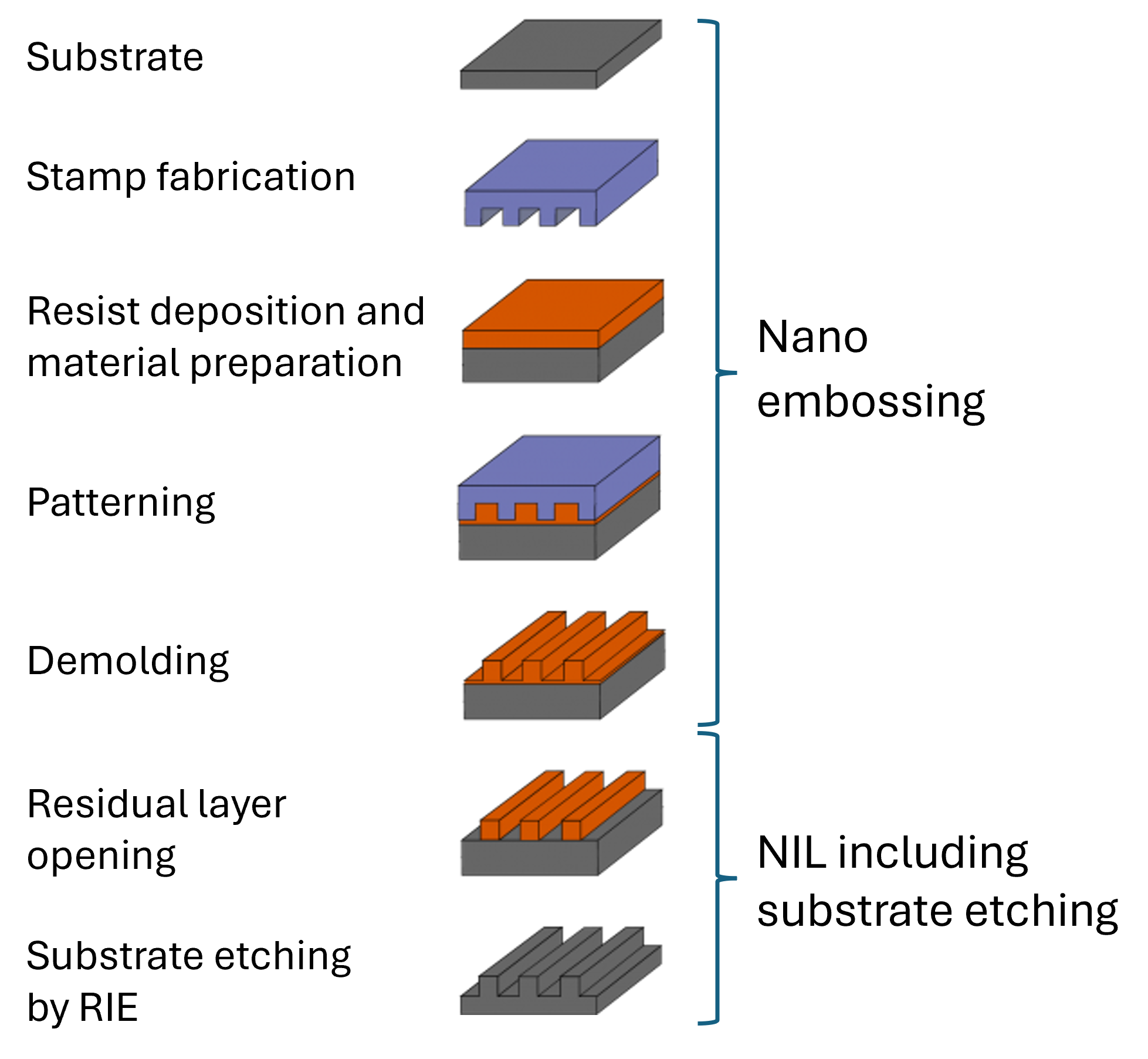
SILSEF’s key technology is Nano Imprint Lithography (NIL) invented in 1995 in the U.S, to reduce the size of microelectronic circuits. It was ranked among the revolutionary technologies by the MIT (“Ten Technologies That can change the world”), thanks to its generic scope and large variety of potential applications.
Schematically, a resist or polymer deposited on the surface of the materia, is embossed with a nano-structured stamp.
Then the pattern can the be transferred into the material by RIE plasma etching using the deformed polymer as a disposable etching mask.
In the traditionnal photo-lithography process, the resist mask is processed by photo insulation through mask. There are limitations related to light interaction with the sides of the masks for nanoscale patterns. Using NIL the resist will be processed by plastic deformation using a hard or soft stamp.
SILSEF develops processes, materials and micro nano patterns to meet its client’s requirements. Along the years, SILSEF tuned various solutions to be able to bring patterning on any material.
We are able to pattern large surfaces (10sx10s of cm) on flat but also on 2.5D (half sphere).
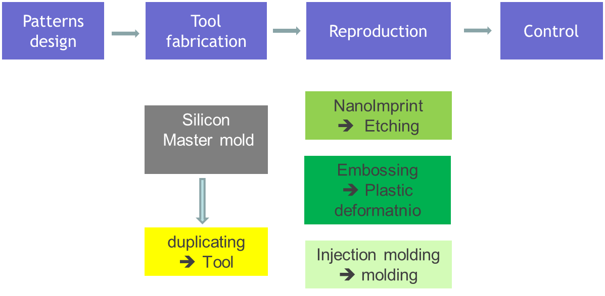 SILSEF is active on the whole process flow, from the design of functional partterns (for optics or wettability) up to control process through dedicated and internally designed characterization equipments to meet your application :
 -
- Design of patterns including simulation and modelling
- Manufacture of tools at micro and nanoscale
- Transfer patterns on a range of materials by etching, plastic deformation moulding or injection moulding
- Geometric and functional characterizations such as wetting proporties or diffraction effects